
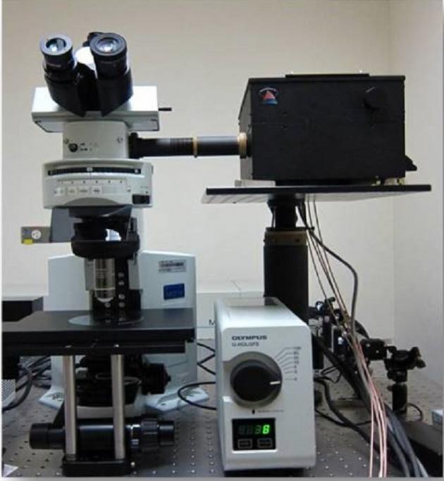


Laser Scanning Confocal Microscope System
JadeMAT
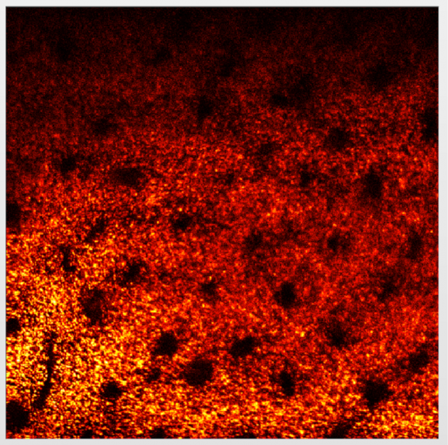
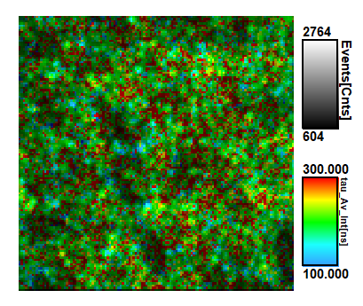
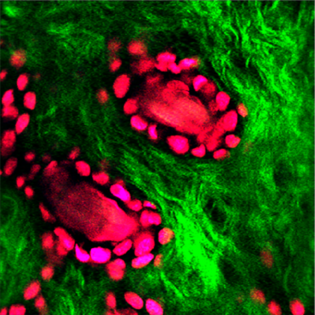
JadeMAT Laser Scanning Confocal Microscope Measurement System can assist researchers doing the micro-scale analysis by using slit and Galvanometer technology and obtain the high resolution micrsope image and spectral measurement result as well. It can be applicable to the field in material analysis, device production, biotechnology and so on. Our system is using modular design whcih can easier for the customers to extend the functions such as PL/EL flourescence spectrum and Raman spectrum, flourescence image, time-resolved photoluminescence (TRPL), fluorescence lifetime imagaing (FLIM), temperature dependent photoluminescence , photocurrent distribution in micro-scale. Moreover, through the 3D surface technology, the system also can do the device surface analysis.
Features
- Spectrum scanning technology for micromteter scale image
- Confocal technology and Galvanometer scanning
- Can also equipped with Raman, PL/EL functions
- Photocurrent scanning for micro-meter scale
- Modular design and advanced integration ability
- Fluorescence measurement and temperature dependent measurement
Application
- Semiconductor materials
- 2D and 3D materials
- Perovskite materials
- Transparent conductive materials
- Solar cell
- Micro LED
Standard Specification (Can be customized)
| Main System | a. Measurement range:400nm-900nm(can be extended) b. PL spectrum range:400nm-1100nm(can be extended ) c. Raman measurement range:100cm-1~4000-1 d. Mapping Core:XY axis Galvanometer scanning e. Mapping method:single direction f. Mapping resolution :<4096x4096, horizontal: 0.35um,vertical: 0.8um g. Mapping speed:1.1 fps / sec.(512 x 512) h. Zoom-in :1-20x i. Dual output switch design: - Photon Counting detector - Spectrometer |
| Excitation Laser | a. Wavelength: 532nm (can be customized) b. FWHM:0.02 nm c. Maximum intensity: > 100 mW |
| Spectrometer | a. Pixel:1650 b. Focal length:328mm c. Grating:300g/mm,1800g/mm d. Detection range:268nm,41nm e. Resolution :0.5nm,0.05nm(1cm-1) f. Measurement range:400nm-1100nm |

 256 bit SSL Encryption